500um
Introduction of a new ultra-thick greyscale positive photoresist

The positive photoresist mr P 22G was developed for greyscale lithography in ultra-thick resist films. The resist enables film thicknesses of 115–140 µm in a single coating step, with double coating up to 200 µm. Due to its low residual absorption after exposure, greyscale patterns up to ~180 µm deep can be produced with a stable operational greyscale working range of ~140 µm.

Exposure wavelengths of 330–420 nm are suitable. Direct write lithography (DWL) is recommended for greyscale patterning. Nearly pixel-free greyscale masks (e.g. HEBS glass based) can also be used.

The 2.5D master structures produced in this way are transferred to materials for permanent use, e.g. by thermal moulding with PDMS and subsequent UV moulding into OrmoComp® or OrmoClear®FX or metallisation, electroplating and replication into OrmoComp® or other suitable materials.

Main applications of the >100 µm deep greyscale master structures are in micro-optics, particularly in free-form optical structures such as lenses, prisms and mirrors for beam shaping and steering. In microfluidics, masters for deep and very deep patterns could also be produced for ‘organ on a chip’ or ‘tumour on a chip’ systems – for drug testing without animal testing.

As part of the OPTIMAL project (https://www.optimal-project.eu/), hierarchical structures were produced in ma-P 22G, i.e. µm and nm scale features were combined in one resist film which, after pattern transfer, could e.g. be used in aviation, with properties for drag reduction and de-icing on the same surface (presented e.g. here: https://mne2025.exordo.com/programme/presentation/194).

In general, mr P 22G enables the fabrication of very deep greyscale patterns using standard-lithography-equipment (laser/LED direct writing, or mask aligner if necessary). Users can thus produce designs themselves and adapt them flexibly – independently of specialised suppliers of resist masters.

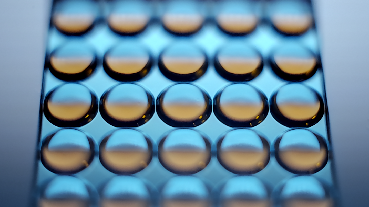
Patterning examples with Direct write lithography (DWL 66+, 405 nm laser):

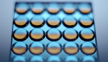
(Patterning and pictures by courtesy of Heidelberg Instruments Mikrotechnik GmbH)


Pattern transfer example: 

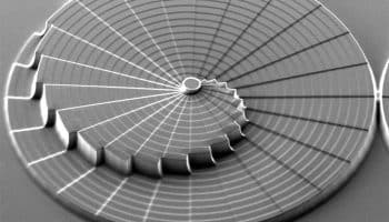
Pattern transfer from a 130 μm high mr-P 22G pattern (a), fabricated at Heidelberg Instruments) by thermal moulding with PDMS, (b) followed by UV moulding with OrmoClear®FX (c)


Hierarchical patterns:

Confocal laser microscope pictures a hierarchical wave structure: 85 µm deep, 280 µm wide by DWL and 400 nm deep, 1 µm wide by LIL on its surface (right: upper ~ 8 µm)

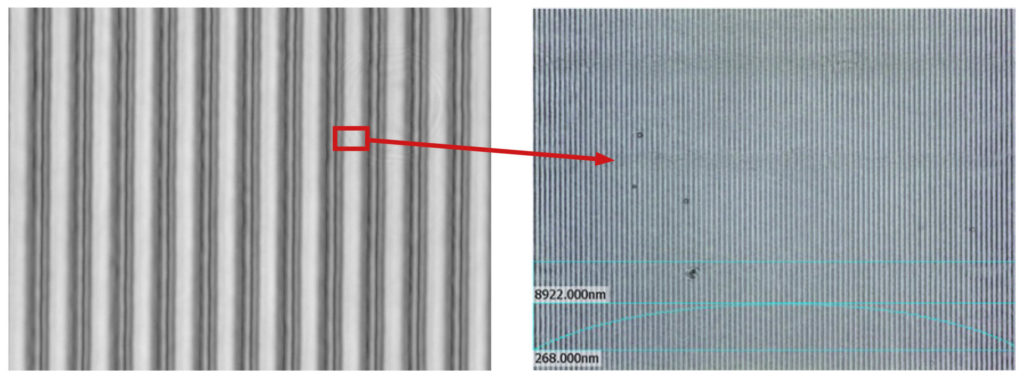
Hierarchical wave structure: 85 µm deep, 280 µm wide (by DWL) and 400 nm deep, 1 µm wide (by laser interference lithography) on its surface (right: upper ~ 8 µm)

positive resist
Grayscale lithography
Micro optics
Wafer level optics
2.5D master structures
Direct write lithography
very deep 2.5 patterns

Contact us.

Anschrift
E-Mail(Required)
Drop files here or
Max. file size: 75 MB.
    Element 32
    0

    Resist Alliance

    micro resist technology is a single entry point for specialty chemicals used in micro and nano manufacturing in Europe. The portfolio of in-house products is complemented by the strategic sales of associated products that are manufactured by our international partners. Here we act as a high-service distributor and offer European medium-sized companies a wide range of complementary products from a single source, which can be used for both established and innovative production and manufacturing processes.

    Kayaku Advanced Materials, Inc. (formerly MicroChem Corp.)

    We offer photoresists and specialty chemicals for MEMS and microelectronic applications from our partner Kayaku Advanced Materials, with whom we have been working for more than 20 years.

    DJ MicroLaminates, Inc.

    We offer dry film resists for MEMS, microfluidics and packaging applications from our partner DJ MicroLaminates, with whom we have been cooperating for over two years.

    Dry Films

    Dry films are ready-to-use polymer films as laminate foil with a high accuracy of the film thickness and excellent adhesion behaviour on various substrates. They are very simple in handling, photo-structurable and both as cut sheets and as roll material available.

    • Available in different film thicknesses
    • UV-crosslinking as negative photoresist
    • Feasibility of high aspect ratios
    • Vertical sidewalls
    • Multi lamination possible – up to 6 layer  complex multi-layer designs
    • High chemical resilience


    • Application as permanent material for optical application (e.g. lenses, wave guides …), in micro fluidics

    Functional materials for inkjet-printing

    Special designed functional materials from the product groups Hybrid Polymers, Photoresists, and Nanoimprint Polymers for the deposition and alternative patterning using inkjet printing process

    • Available in different viscosities (adjustable)
    • Suitable in commercial inkjet printing devices
    • Focused on high reliability of droplet generation
    • UV-curable formulations


    • Usable as a permanent material for optical application (e.g. lenses, wave guides, optical couplers, diffractive elements, …)
    • Packaging material in the micro electronic
    • Deposition / patterning on substrates with surface topography
    • Imprint material for nano-structuring with high dose accuracy

    Nanoimprint Resists

    Nanoimprint Lithography (NIL) is a straight forward, low cost, and high throughput capable technology for the fabrication of nanometer scaled patterns. Main application fields are photonics, next generation electronics, as well as bio- and sensor applications.

    micro resist technology GmbH has provided tailor-made resist formulations for nanoimprint lithography (NIL) since 1999. The unique key features of our products are outstanding film forming and imprinting performance beside excellent pattern fidelity and plasma etch stability. Besides our highly innovative material developments in close contact to industrial needs, our strength is the ability to adjust our materials in film thickness as well as addressing certain needs of the specific use cases within the formulation. Our nanoimprint resists are mostly applied as an etch mask for pattern transfer into various substrates, like Si, SiO2, Al or sapphire.

    Our portfolio covers materials for the classical thermal NIL (T-NIL), in which a thermoplastic polymer is used, as well as UV-NIL, in which a liquid formulation is photo crosslinked upon photo exposure. With our technological expertise and know-how we are able to find the right material for your process and applications. Please contact us for your technical support!

    Hybrid Polymers

    micro resist technology offers a broad portfolio of UV-curable hybrid polymer products for micro-optical applications. Their excellent optical transparency and high thermal stability makes them perfectly suitable for the production of polymer-based optical components and waveguides. The main fields of application are micro lenses, diffractive optical elements (DOE), gratings, and single-mode or multi-mode waveguides.

    OrmoComp®: DE 30 210 075 433; IR 1 091 982 ; TW 100030626; OrmoClear®: DE 30 210 075 434; IR 1 091 359 ; TW 100030628; OrmoStamp®: DE 30 210 075 435; IR 1 092 621 ; TW 100030629; OrmoPrime®: DE 30 210 075 436

    Positive Photoresists

    Positive Photoresists for UV lithography (mask aligner, laser, greyscale exposure) and e-beam lithography

    • Variety of viscosities for 0.1 µm – 60 µm film thickness in one spin-coating step
    • Effective for broadband, g-line, h-line or i-line exposure, laser direct writing at 350…450 nm and e-beam lithography
    • No post exposure bake
    • Easy removal
       
    • For pattern transfer: Etch mask, mould for electroplating, mould for UV moulding
    • Use in microsystems technology, microelectronics, micro-optics – manufacture of e.g. MEMS, LEDs, ICs, MOEMS, fiber optics telecommunications devices, flat panel displays

    Negative Photoresists

    Photoresists for UV (mask aligner, laser)/ DUV and e-beam lithography

    • Effective for broadband and i-line, Deep UV, e-beam exposure, or laser direct writing @ 405 nm
    • Lift-off resists with tunable pattern profile, high temperature stability up to 160 °C
    • Variety of viscosities for different film thicknesses in one spin-coating step
       
    • For pattern transfer: Physical vapour deposition (PVD) and single  layer lift-off, etch mask, mould for electroplating
    • For permanent applications: Polymeric waveguides
    • Use in microsystems technology, microelectronics, micro-optics  – manufacture of e.g. LEDs, ICs, MEMS, flat panel displays, fiber optics telecommunications devices