
Career

Bild1n
New: 200 mm Lithography and new Nanoimprint Capabilities in our Cleanroom
26.06.2026

In 2026, micro resist technology significantly expanded its cleanroom capabilities towards 200 mm wafer processing while also extending nanoimprint lithography capabilities to full-area processing on substrates up to 150 mm. This upgrade enables advanced processing on industry-relevant substrate sizes and opens new opportunities for customer projects, process development, and material evaluation.

Extended Lithography Capabilities up to 200mm

Our lithography infrastructure now supports substrates up to 200 mm in diameter, extending our previous capabilities. Exposure is provided by two complementary mask aligner platforms: an established SUSS MA6 system (Hg lamp-based) and now, in addition, the LED-based exposure tool EVG 6200NT with wavelengths at 365 nm, 405 nm, and 435 nm. At the same time, a 200 mm-compatible spin coater has been installed.

This combination increases flexibility in resist processing, improves tool availability, and enables direct comparison between LED and Hg lamp exposure, allowing systematic studies of exposure performance, process latitude, and resist sensitivity across different illumination concepts.
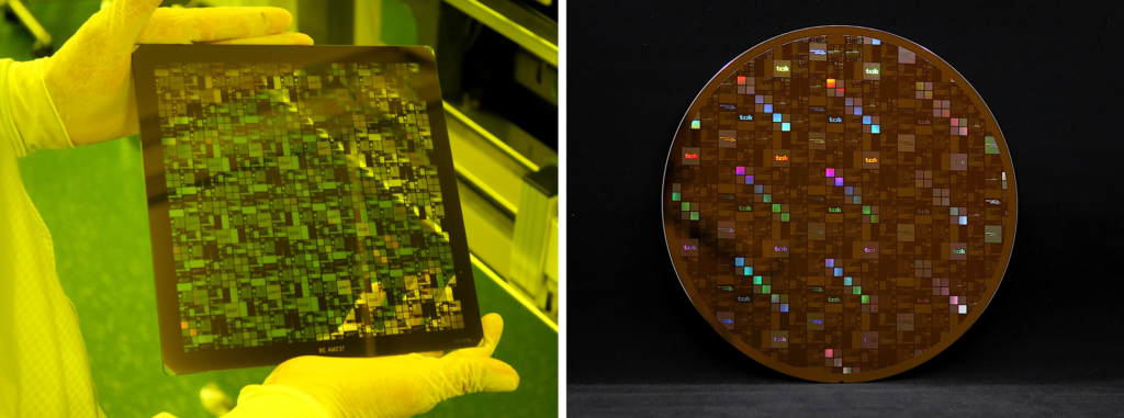
Fig. 1: Left: 9-inch MRT UV-mask with different test patterns. Right: Fully exposed 200 mm wafer coated with ma-P 1215 photoresist, demonstrating the exposure capability

Integrated Nanoimprint Capability
In addition to photolithography, nanoimprint lithography (NIL) capabilities have been further expanded by the EVG 6200NT tool. Alongside our established compact nanoimprint tools (NILT CNI) for rapid feasibility studies and pre-tests, the additional SmartNIL® imprint platform enables:

  • UV-based, low-pressure imprinting with high uniformity and controlled resist flow
  • full-area imprinting on substrates up to 150 mm
  • in-tool fabrication of flexible working stamps using polymer films (e.g., PC foil)
  • rapid prototyping and evaluation of imprint processes

This combination allows efficient screening on compact tools followed by transfer to larger-area imprint processes.
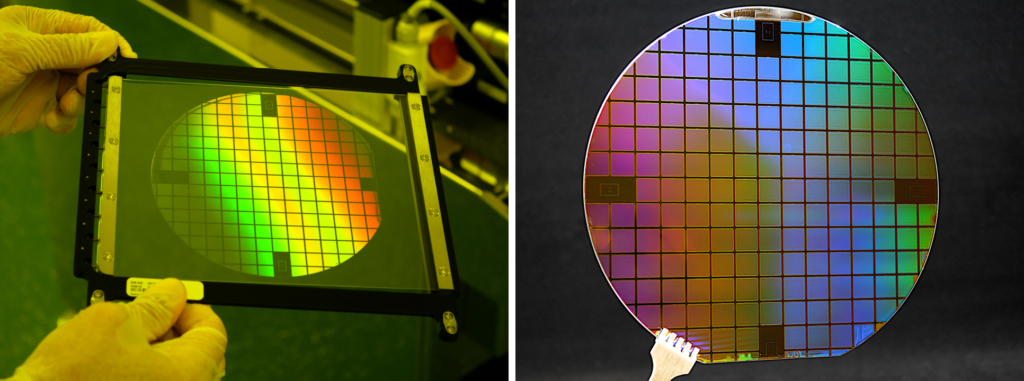
Fig. 2: Left: Flexible imprint stamp fabricated directly in the tool with Optool PS91 stamp polymer. Right: Full-area imprint performed in mr-NIL213FC resist, showing uniform pattern transfer on 150mm wafer

The combination of 200 mm mask alignment, multi-wavelength LED exposure, and full-field nanoimprint lithography significantly strengthens our cleanroom infrastructure. It enables more comprehensive process development, improved benchmarking of exposure technologies and new application fields for NIL materials.
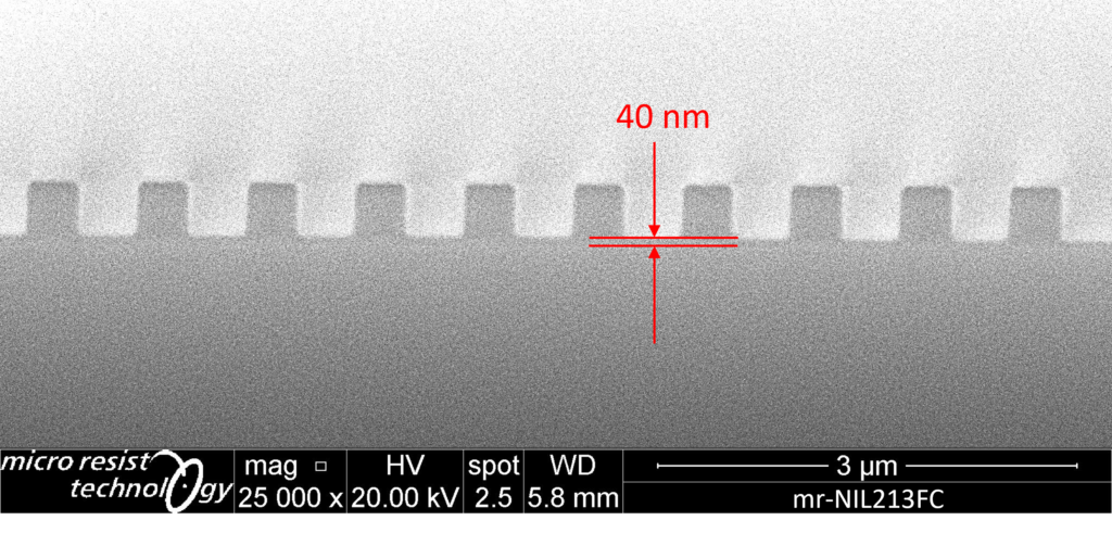
Fig. 3: Tilted SEM image of a 400 nm line-and-space pattern in mr-NIL213FC created via imprint lithography in our SmartNIL® tool with a measured residual layer thickness of approximately 40 nm

The expansion of lithography and nanoimprint capabilities is also a key component of the establishment of the European “Center of Excellence for Technology & Innovation” in Berlin as part of the global TOK Group

Nanoimprint Resist
Positive Resist
Negative Resist
UV-Lithography
Nanoimprint Lithography
Dry film resists
UV-NIL
Dry Etch Mask

Contact us.

Element 32
0

Resist Alliance

micro resist technology is a single entry point for specialty chemicals used in micro and nano manufacturing in Europe. The portfolio of in-house products is complemented by the strategic sales of associated products that are manufactured by our international partners. Here we act as a high-service distributor and offer European medium-sized companies a wide range of complementary products from a single source, which can be used for both established and innovative production and manufacturing processes.

Kayaku Advanced Materials, Inc. (formerly MicroChem Corp.)

We offer photoresists and specialty chemicals for MEMS and microelectronic applications from our partner Kayaku Advanced Materials, with whom we have been working for more than 20 years.

DJ MicroLaminates, Inc.

We offer dry film resists for MEMS, microfluidics and packaging applications from our partner DJ MicroLaminates, with whom we have been cooperating for over two years.

Dry Films

Dry films are ready-to-use polymer films as laminate foil with a high accuracy of the film thickness and excellent adhesion behaviour on various substrates. They are very simple in handling, photo-structurable and both as cut sheets and as roll material available.

  • Available in different film thicknesses
  • UV-crosslinking as negative photoresist
  • Feasibility of high aspect ratios
  • Vertical sidewalls
  • Multi lamination possible – up to 6 layer  complex multi-layer designs
  • High chemical resilience


  • Application as permanent material for optical application (e.g. lenses, wave guides …), in micro fluidics

Functional materials for inkjet-printing

Special designed functional materials from the product groups Hybrid Polymers, Photoresists, and Nanoimprint Polymers for the deposition and alternative patterning using inkjet printing process

  • Available in different viscosities (adjustable)
  • Suitable in commercial inkjet printing devices
  • Focused on high reliability of droplet generation
  • UV-curable formulations


  • Usable as a permanent material for optical application (e.g. lenses, wave guides, optical couplers, diffractive elements, …)
  • Packaging material in the micro electronic
  • Deposition / patterning on substrates with surface topography
  • Imprint material for nano-structuring with high dose accuracy

Nanoimprint Resists

Nanoimprint Lithography (NIL) is a straight forward, low cost, and high throughput capable technology for the fabrication of nanometer scaled patterns. Main application fields are photonics, next generation electronics, as well as bio- and sensor applications.

micro resist technology GmbH has provided tailor-made resist formulations for nanoimprint lithography (NIL) since 1999. The unique key features of our products are outstanding film forming and imprinting performance beside excellent pattern fidelity and plasma etch stability. Besides our highly innovative material developments in close contact to industrial needs, our strength is the ability to adjust our materials in film thickness as well as addressing certain needs of the specific use cases within the formulation. Our nanoimprint resists are mostly applied as an etch mask for pattern transfer into various substrates, like Si, SiO2, Al or sapphire.

Our portfolio covers materials for the classical thermal NIL (T-NIL), in which a thermoplastic polymer is used, as well as UV-NIL, in which a liquid formulation is photo crosslinked upon photo exposure. With our technological expertise and know-how we are able to find the right material for your process and applications. Please contact us for your technical support!

Hybrid Polymers

micro resist technology offers a broad portfolio of UV-curable hybrid polymer products for micro-optical applications. Their excellent optical transparency and high thermal stability makes them perfectly suitable for the production of polymer-based optical components and waveguides. The main fields of application are micro lenses, diffractive optical elements (DOE), gratings, and single-mode or multi-mode waveguides.

OrmoComp®: DE 30 210 075 433; IR 1 091 982 ; TW 100030626; OrmoClear®: DE 30 210 075 434; IR 1 091 359 ; TW 100030628; OrmoStamp®: DE 30 210 075 435; IR 1 092 621 ; TW 100030629; OrmoPrime®: DE 30 210 075 436

Positive Photoresists

Positive Photoresists for UV lithography (mask aligner, laser, greyscale exposure) and e-beam lithography

  • Variety of viscosities for 0.1 µm – 60 µm film thickness in one spin-coating step
  • Effective for broadband, g-line, h-line or i-line exposure, laser direct writing at 350…450 nm and e-beam lithography
  • No post exposure bake
  • Easy removal
     
  • For pattern transfer: Etch mask, mould for electroplating, mould for UV moulding
  • Use in microsystems technology, microelectronics, micro-optics – manufacture of e.g. MEMS, LEDs, ICs, MOEMS, fiber optics telecommunications devices, flat panel displays

Negative Photoresists

Photoresists for UV (mask aligner, laser)/ DUV and e-beam lithography

  • Effective for broadband and i-line, Deep UV, e-beam exposure, or laser direct writing @ 405 nm
  • Lift-off resists with tunable pattern profile, high temperature stability up to 160 °C
  • Variety of viscosities for different film thicknesses in one spin-coating step
     
  • For pattern transfer: Physical vapour deposition (PVD) and single  layer lift-off, etch mask, mould for electroplating
  • For permanent applications: Polymeric waveguides
  • Use in microsystems technology, microelectronics, micro-optics  – manufacture of e.g. LEDs, ICs, MEMS, flat panel displays, fiber optics telecommunications devices